 |
|||
|
|
|||
|
Page Title:
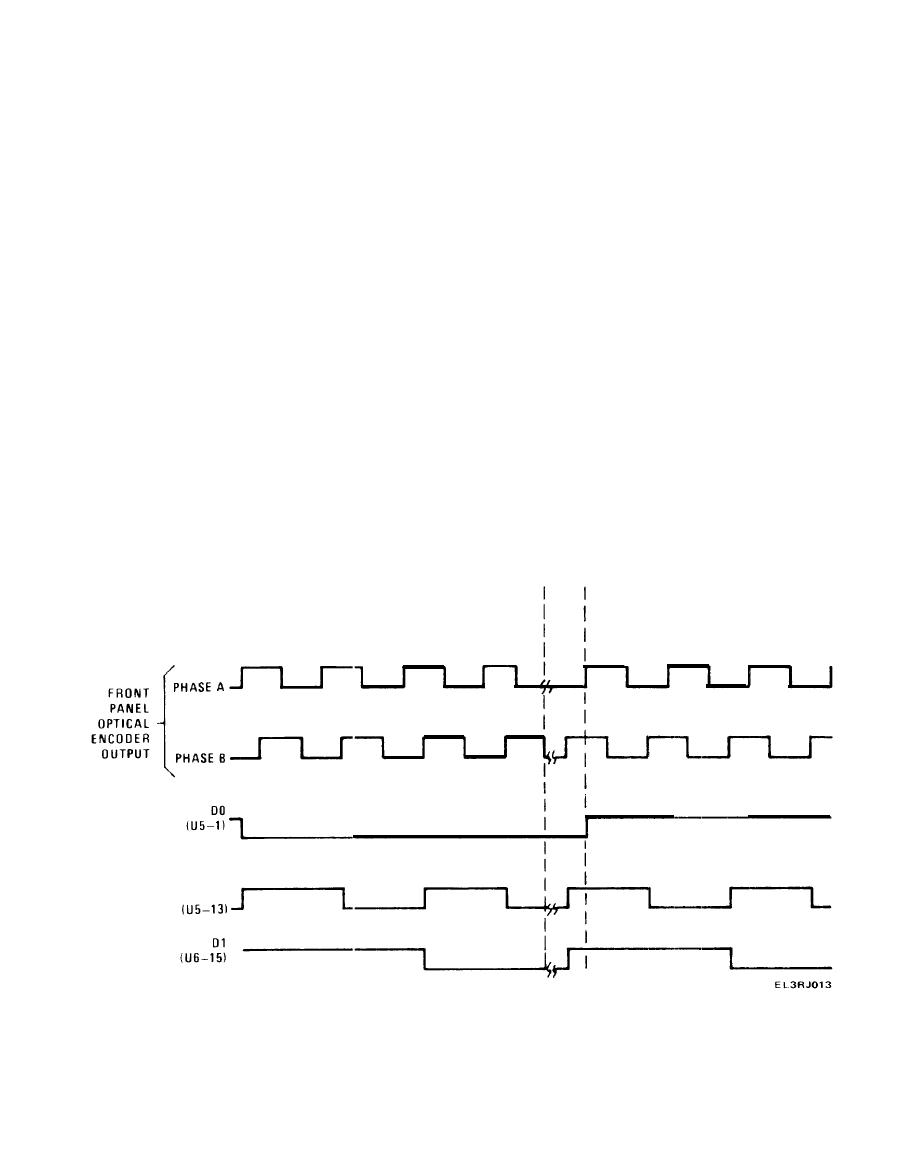
Figure 5-10. Manual Tuning Timing Diagram |
|
||
| ||||||||||
|
|
 TM 11-5865-215-13
conversion circuits on CCA A3. The A-quad-B conversion circuits then
convert the PHASE A and PHASE B signals to binary data (see figure
FO-10).
D flip-flops U5A and U5B, together with JK flip-flop U6B, comprise
the A-quad-B circuit and convert the PHASE A and PHASE B pulse inputs
from the front panel optical encoder (MANUAL TUNING control) into
binary data (see figure 5-10). These data change the frequency field
of the receiver control receiver command (51 bit) word. When the
MANUAL TUNING control is rotated clockwise, the PHASE A pulses lead
the PHASE B pulses. This causes flip-flop U5A to reset, providing a
0 (increase frequency) bit to the DO port of output register U11B.
The PHASE B input also clocks flip-flops U5B and U6B to produce pulse
inputs to the D1 port of output register U11B. The pulse rate of this
input is proportional to the rate at which the MANUAL TUNING control
is rotated. Counterclockwise rotation of the MANUAL TUNING control
causes U5A to set. This produces a high 1 (decrease frequency) bit
input to register U11B. Again, the pulse output rate is determined by
the speed at which the MANUAL TUNING control is rotated. An active
(low) output port 7 OB73 bit transfers the MANUAL TUNING data in reg-
ister U11B to the respective IB20 and IB21 lines of microprocessor
input port 2.
Manual Tuning Timing Diagram
5-27
|
|
Privacy Statement - Press Release - Copyright Information. - Contact Us |