 |
|||
|
|
|||
|
|
|||
| ||||||||||
|
|
 TM 11-5865-215-13
sequence T2). Decoders U11 and U3A thru U3D translate the
timing
format
command into a counter preset value as shown in table 5-7
(logic
shown is positive true). This preset value determines the
number
of receiver command bits transferred during the output cycle.
The Q2 and Q3 outputs of format counter U2, together with the Q1
and Q0 outputs of format counter Ul, address RAM U26 via RAM address
multiplexer U18. The resulting 4-bit RAM output character is applied
to parallel-to-serial converter U10. The converter responds to format
Q0 output of counter U2 and the Q counter U2 and Ul outputs by trans-
ferring each 4-bit character, one bit at a time, into the serial re-
ceiver command data stream. These data are transferred to the SDU
display and receiver via line drivers U23A and U23B, respectively. Or,
if computer format is selected, the data are transferred to the com-
puter via line driver U32B. The 6.5-kHz clock driving the format
counters is also applied to the receiving units via NAND gate U15C,
drivers U29B and U30F, and line drivers U16A, U16B and U24B.
(3) Timing sequence T6. When the next-to-last serial data bit
is clocked out of output interface CCA AS, the C0 (pin 7) output of
format counter U1 drops low. This low sets output load latch U14B,
and resets write timer (8) to zero and holds the counter at zero.
(4) Timing sequence T7. As the last receiver command data bit
is clocked out, the format counter C0 output (from U-7) goes high.
This high output combines with the high output from output load latch
U14B (pin 9) to enable NAND gate U15B. U15B responds to the inverted
clock input (via U7A) to produce a negative pulse at U15B (pin 6),
which resets output latch U14D. The resulting low output of the re-
set latch inhibits clock gate U5A and switches RAM address multiplexer
U18 once again allowing RAM U26 to be addressed by microprocessor out-
put port 3 (OB30 thru 0B33 at CCA A5 pins 25 thru 28).
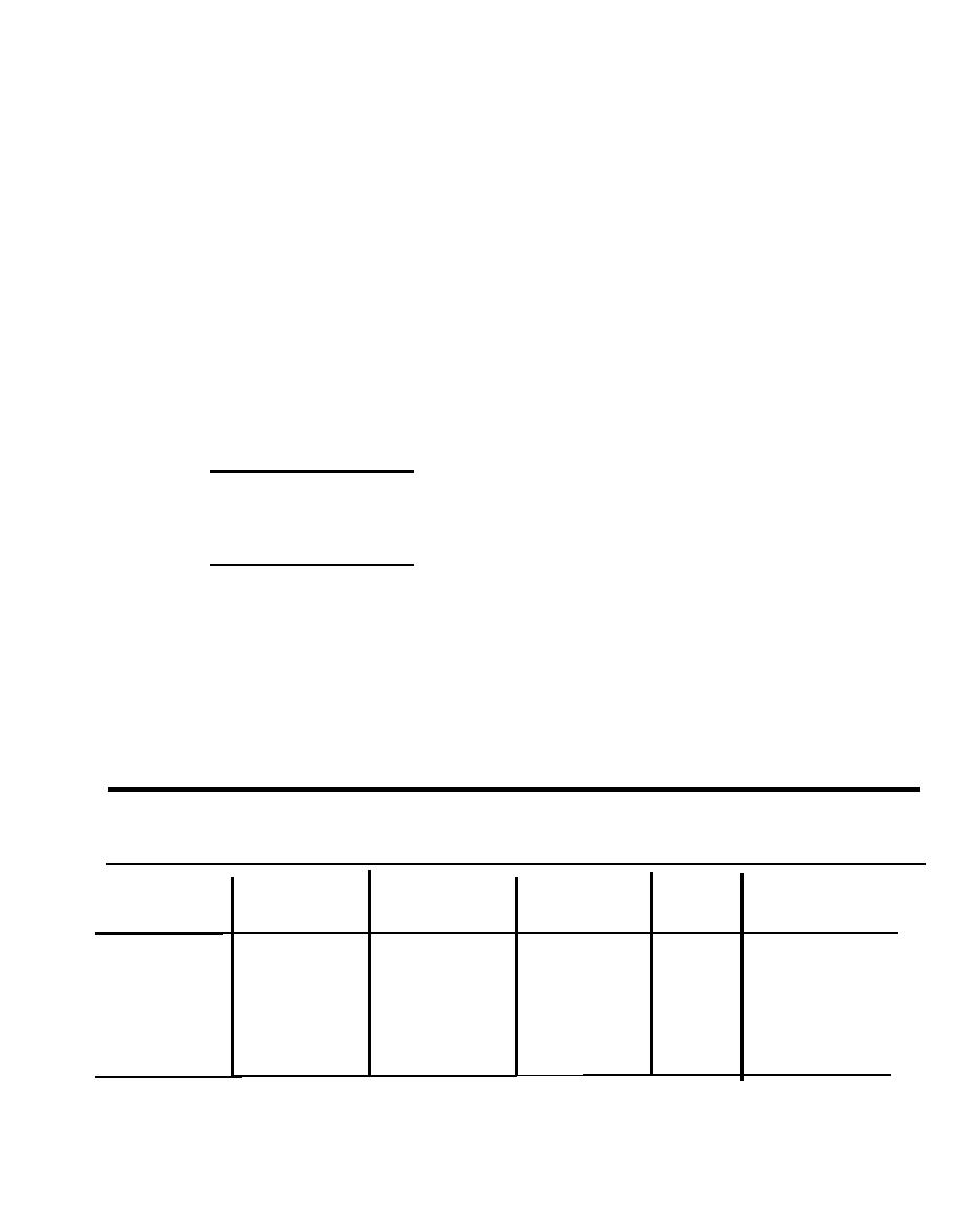
Output Format
Format counter
Output format
command (loaded
Number
preset value
during T2)
of bits
trans-
A5U2
A5U1
OB40
OB41
Destination
ferred
P3 P2 P1 P0
P3 P2 P1 P0
(A5 pin 30)
(A5 pin 31)
52*
Receiver or
0011
0011
0
1
SDU
64
Computer
0000
0100
1
1
*The first bit transferred is not used.
5-33
|
|
Privacy Statement - Press Release - Copyright Information. - Contact Us |
|
|
Integrated Publishing, Inc. - A (SDVOSB) Service Disabled Veteran Owned Small Business
|

